Writing a Ghidra processor module
14 Feb 2025 by Jonas Rudloff
In this article we will create a Ghidra processor module for the iRISC processors, these processors are embedded in the ConnectX series of NICs from NVIDIA/Mellanox.
A more complete version of a Ghidra processors module for iRISC is available here[1]
What we know about iRISC:
This following is the condensed knowledge of our previous two blog posts where we analysed the firmware and found SHA256:
- Is it a big endian processor
- Similar instruction layout to the MIPS architecture: 6 bits opcode, 5 bits per register.
- load and store instruction does not have same encoding of the offset.
- load and store instruction have something weird going on in the low bits of the offset.
- The iRISC has 64 bit registers.
r1is the stack pointerr19-r20are callee saved registers.r4-??: function parameter registers.opcode = 0x00: Add immediate instruction,add rd, rs, imm16.opcode = 0x19: Load instruction.opcode = 0x1b: Store instruction.opcode = 0x1c: Store instruction, but adds offset to base address register.opcode = 0x3f: Used for return, and other things.opcode = 0x06,0x07,0x08,0x09: sets 16bit words inside 64bit registers.opcode = 0x1e: might be a 64 bit store operation.opcode = 0x25: Is a jump/call instruction.opcode = 0x05: Does some kind of comparison operation.opcode = 0x29: is a conditional branch with 16bit offset.opcode = 0x3f, subop=0x000:add-instruction.opcode = 0x3f, subop=0x008:or-instruction.opcode = 0x3f, subop=0x00a:and-instruction.opcode = 0x3f, subop=0x00e:xor-instruction.opcode = 0x3f, subop=0x081:shr-instruction.opcode = 0x3f, subop=0x083:shl-instruction.
We also know the following instruction layouts
R-type:  |  6bit opcode  |  5bit rs  |   5bit rd   |   5bit rt   | 11bit immidiate |
I-type:  |  6bit opcode  |  5bit rs  |   5bit rd   |        16bit immidiate        |
ST-type: |  6bit opcode  |  5bit rs  | 5bit hi-off |   5bit rt   |   11bit lo-off  |
J-type:  |  6bit opcode  | 2bit jmpop |             24bit jump-offset              |
SH-type  |  6bit opcode  |  5bit rs  |   5bit rd   |   5bit shamt |   11bit funct  |
Ghidra SLEIGH
Ghidra supports for disassembling different architecture is based on a DSL called SLEIGH, every architecture that Ghidra supports has a corresponding processor module[2] which is primarily SLEIGH code and a bit of XML as glue.
Documentation is available in the Ghidra repository, and we have made a copy available here
The XML files contains basic information about the architecture:
- The name, description, and ID
- Information about different variants of instructions set, such as extensions, endianness,
- Compiler specific information like common stack pointers, frame pointers, and other parts of the calling convention, and alignment hints for structure layout.
SLEIGH consists has three different constructs ‘defines’, ‘attachments`, ‘tables’.
- ‘Defines’: Defines certain things about the ISA such as: Endianness, Alignment, Registers, Tokens, and Token Fields, and how these relate to each other.
- ‘Attachments’: Are used for attaching values(addspress space locations or numbers) to token fields.
- ‘Tables’: Describes the decoding of diffrent instructions, their presentation in disassembly, and their semantics.
Our Processors Module
We will ignore the XML files, they are important but not really that interesting. They are available here
define endian=big;

define alignment=4;

define space ram type=ram_space size=4 default;
define space register type=register_space size=4;
This declares that the iRISC is a big endian machine with 4 bytes of alignment as well as two address spaces: one for registers and one for our main memory.
Next we will go ahead and define our registers:
define register offset=0x00000 size=8 [
    zero r1 r2 r3 r4 r5 r6 r7
    r8 r9 r10 r11 r12 r13 r14 r15
    r16 r17 r18 r19 r20 r21 r22 r23
    r24 r25 r26 r27 r28 r29 r30 r31
];

define register offset=0x00000 size=4 [
    zeroh zerol r1h r1l r2h r2l r3h r3l r4h r4l r5h r5l r6h r6l r7h r7l
    r8h r8l r9h r9l r10h r10l r11h r11l r12h r12l r13h r13l r14h r14l r15h r15l
    r16h r16l r17h r17l r18h r18l r19h r19l r20h r20l r21h r21l r22h r22l r23h r23l
    r24h r24l r25h r25l r26h r26l r27h r27l r28h r28l r29h r29l r30h r30l r31h r31l
];
This declares 32 64bit registers: zero, r1-r31 that overlaps with 32 pairs of 32bit registers each of which consists of the high and low register. These are our general purpose registers.
Next we can define our token(s) and their fields, in our case there will only be a single token as every instruction is excatly 4 bytes long:
define token instr(32)
    op=(26, 31)
    rs=(21, 25)
    rshi=(21, 25)
    rslo=(21, 25)
    brop1=(21, 25)
    jmpop=(24, 25)
    imm24=(0, 23)
    simm24=(0, 23) signed
    rd=(16, 20)
    rdhi=(16, 20)
    rdlo=(16, 20)
    cmpop=(16, 20)
    brop2=(16, 20)
    rt=(11, 15)
    rthi=(11, 15)
    rtlo=(11, 15)
    shamt=(11, 15)
    imm16=(0, 15)
    imm11=(0, 10)
    simm16=(0, 15) signed
    funct=(0, 8)

    off14=(2, 15) signed
    off15=(1, 15) signed
    off11=(0, 10) signed

    stoff_hi=(16, 20) signed
    stoff14_lo=(2, 10)
;
In this definition we define a token called instr which is 32bits long, this token consists of multiple possible overlapping fields.
Then we can attach the registers to the token fields describing them:
attach variables [ rd rs rt ] [
    zero r1 r2 r3 r4 r5 r6 r7
    r8 r9 r10 r11 r12 r13 r14 r15
    r16 r17 r18 r19 r20 r21 r22 r23
    r24 r25 r26 r27 r28 r29 r30 r31
];

attach variables [ rdhi rshi rthi ] [
    zeroh r1h r2h r3h r4h r5h r6h r7h
    r8h r9h r10h r11h r12h r13h r14h r15h
    r16h r17h r18h r19h r20h r21h r22h r23h
    r24h r25h r26h r27h r28h r29h r30h r31h
];

attach variables [ rdlo rslo rtlo ] [
    zerol r1l r2l r3l r4l r5l r6l r7l
    r8l r9l r10l r11l r12l r13l r14l r15l
    r16l r17l r18l r19l r20l r21l r22l r23l
    r24l r25l r26l r27l r28l r29l r30l r31l
];
This means that when we are talking about rd, rs or rt they no longer behave like regular numbers but instead whatever they are attached to. This means that if rt=5 we are really talking about r5, so an operation like rd = rs + rt will read whatever rs and rt is pointing to, and add those numbers together and write the result to whatever rd is pointing to. In constrast the expression, rd = rs + simm16 will only read what rs is pointing to, but simm16 will just be the bits from the instruction.
Finaly we can begin making our tables. We start by makeing a few subtables, for fixing the zero register.
RD: rd is rd { export rd; }

RSsrc: rs is rs { export rs; }
RSsrc: rs is rs & rs=0 { export 0:8; }

RTsrc: rt is rt { export rt; }
RTsrc: rt is rt & rt=0 { export 0:8; }
This will make it so that if rs or rt is the constant 0, we will not read the zero register but instead be the constant 0.
However this does not override the meaning of rs and rt but introduces 2 subtables RSsrc and RTsrc which does what we want.
The way tables in general works is the following:
<table name> : <disassembly display> is <list of constraints> [ <disassembly expressions> ] { <semantics> }
- Table name: This is the name of the Table, and for the root(‘instruction’) table this is left empty.
- Disassembly display: this is what is displayed in the disassembly view.
- Constraints: Speficies the matching of token fields.
- Disassembly expressions: Simple calculation, resulting in disassembly variables, which can both be used in the disassembly display or in the semantics. This can be used for coaleasing offsets that are spread over multiple token fields, as is the instance for the offset in our store instruction.
- Semantics: Describes what the table is supposed to.
Next we will make our first instruction, and it will be a catch-all instruction without any constraints:
define pcodeop UnkOp;

:unk.^op RD, RSsrc, RTsrc, imm16 is op & RD & RSsrc & RTsrc & imm16 {
    RD = UnkOp(op:1, RSsrc, RTsrc);
}
This will make is no that any instruction that ghidra otherwise can’t decode will be decoded as instruction that looks like: unk.0x42 r1, r2, r3, 0x1337
A few things to notice here:
^: simply a means to concatanate the two expressions without a space between them.UnkOp: A custom PCODE operation that Ghidra will treat as opaque and only use for dataflow analysis.op:1: castop, which is a 6bit token field to a 1 byte number. Ghidra primarily deals in byte-sized numbers.- No constraints: Even as we don’t have any constraints on the instruction we still need to list which token field we want to use.
- Sub-tables: We are using the
RSsrc,RTsrc,RDtables we made before, and notrd,rs, andrtdirectly. - Tables are matched by matching the most specific constructor, this means that constructors must either be fully contained in the a diffrent constructor’s constraints or be fully seperate from it. This is detailed in the SLEIGH manual
Trying our processor module
- Symlink the processor module into ghidra:
ln -s /path/to/custom/module /path/to/ghidra/Ghidra/Processor/iRISC - Create a new project, and import
IRON_PREP_CODE - Choose the iRISC language
- Open the Ghidra CodeBrowser, and do not auto analyse.
- press
dat the top of the disassembly view.
We now have the following:
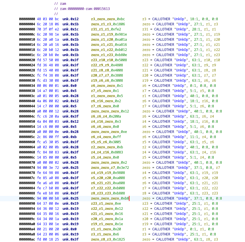
This is basically where we started when we began writing our python disassembler. However as we have more knowlegde we can just simply implement this knowlegde in the SLEIGH language
Improving our SLEIGH module: ALU instructions
Next we will make a few other opcodes:
:add RD, RSsrc, simm16          is op=0x00 & RD & RSsrc & simm16 {
    RD = RSsrc + simm16;
}

:set0 RD, RSsrc, imm16          is op=0x06 & RD & RSsrc & imm16 {
    RD = (RSsrc & 0x0000ffffffffffff) | (imm16 << 48);
}

:set1 RD, RSsrc, imm16          is op=0x07 & RD & RSsrc & imm16 {
    RD = (RSsrc & 0xffff0000ffffffff) | (imm16 << 32);
}

:set3 RD, RSsrc, imm16          is op=0x08 & RD & RSsrc & imm16 {
    RD = (RSsrc & 0xffffffffffff0000) | (imm16 << 0);
}

:set2 RD, RSsrc, imm16          is op=0x09 & RD & RSsrc & imm16 {
    RD = (RSsrc & 0xffffffff0000ffff) | (imm16 << 16);
}
Some things of note here:
op=0x00: We are now using constraints to match instruction based on opcodessimm16: we are using a sign-extended version of the low 16bits.- Semantics: Can be complex expressions with a lot of operations.
set3andset2: is in the ‘wrong’ order: This is just how the iRISC works, nothing we can do about that. Only NVIDIA/Mellanox knows the reason for this.
So far we have only dealt with instructions of the form:
foo <reg>, <reg>, <constant>
next we will deal with some of the reg-reg-reg type instructions:
define pcodeop UnkAlu;

:alu.^funct RD, RSsrc, RTsrc    is op=0x3f & funct & RD & RSsrc & RTsrc {
    RD = UnkAlu(funct:2, RSsrc:8, RTsrc:8);
}

:add RD, RSsrc, RTsrc           is op=0x3f & funct=0x000 & RD & RSsrc & RTsrc {
    RD = RSsrc + RTsrc;
}

:or  RD, RSsrc, RTsrc           is op=0x3f & funct=0x008 & RD & RSsrc & RTsrc {
    RD = RSsrc | RTsrc;
}

:mv  RD, RTsrc                  is op=0x3f & funct=0x008 & RD & RTsrc & rt=rs {
    RD = RTsrc;
}

:and RD, RSsrc, RTsrc           is op=0x3f & funct=0x00a & RD & RSsrc & RTsrc {
    RD = RSsrc & RTsrc;
}

:xor RD, RSsrc, RTsrc           is op=0x3f & funct=0x00e & RD & RSsrc & RTsrc {
    RD = RSsrc ^ RTsrc;
}

:shl RDlo, RSlosrc, shamt       is op=0x3f & funct=0x081 & RDlo & RSlosrc & shamt {
    RDlo = RSlosrc << shamt:1;
}

:shr RDlo, RSlosrc, shamt       is op=0x3f & funct=0x083 & RDlo & RSlosrc & shamt {
    RDlo = RSlosrc >> shamt:1;
}
Things to note here:
- Another catch-all instruction
alu.^funct mv: Is really just anorinstruction wherert=rs, this gives nicer disassembly.RDlo,RSlosrc: Similar tables toRDandRSsrcbut only working on the low part of the registers.
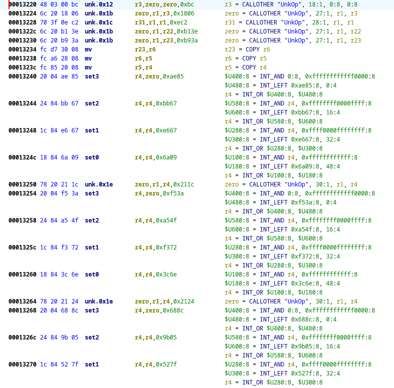
At this point in time our disassembly for the SHA256_init looks like this
We still have much more to do…
More instructions: Memory operations
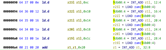
We start with the load instruction:
LDOFF14: offset                 is off14 [ offset = off14 << 2; ] {
    export *[const]:4 offset;
}

:ld.d RDlo RSlosrc, LDOFF14     is op=0x19 & RDlo & RSlosrc & LDOFF14 {
    RDlo = *[ram]:4 (RSlosrc + LDOFF14);
}
There are many things going on here:
- We have a subtable(
LDOFF14) for calcualting the load offset(rememeber the 2 low bits being weird?) - This sub table is using ‘disassembly expressions’, which are calculations which happens at disassembly time and not when the instruction is executed:
[ offset = off14 << 2; ]. - The semantics of that subtable is also a bit complicated, but in essence we casting a disassembly veriable(
offset) to a constant value with a certain size of bytes by dereferenceing a address space that is an idintity map of values. - The way
LDOFF14is displayed is the result of the calulationoff14 << 2because we are displayingoffset, this means that ifimm16is0x0016thenoff14will be0x0005because we have discarded the 2 low bits, and thenoffsetwill be calculated to be0x0014which is the final value that we will both displayed and exported. - The instruction
ld.duses that theLDOFF14subtable - The semantics of
ld.ddereferances theramaddress space with a 4 byte access.
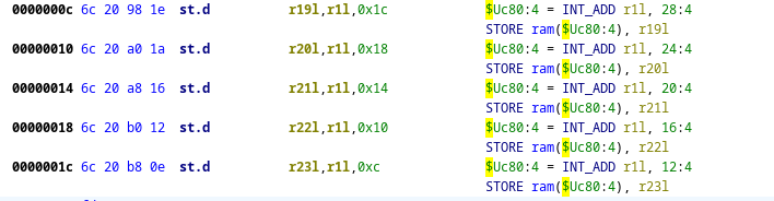
The st.d instruction is simmilar, except that the offset is split between multiple token fields:
STOFF14: offset                 is stoff_hi & stoff14_lo [ offset = (stoff_hi << 11) | (stoff14_lo << 2); ] {
    export *[const]:4 offset;
}

:st.d RTlosrc, RSlosrc, STOFF14  is op=0x1b & RTlosrc & RSlosrc & STOFF14 {
    *[ram]:4 (RSlosrc + STOFF14) = RTlosrc;
}

:st.d! RTlosrc, RSlosrc, STOFF14 is op=0x1c & RTlosrc & RSlosrc & STOFF14 {
    *[ram]:4 (RSlosrc + STOFF14) = RTlosrc;
    RSlosrc = RSlosrc + STOFF14;
}
More instructions: Function entry and return
This time we nned to fix the following instructions:
unk.0x12 r3, zero, zero, 0xbc: This you read the return address and store it inr3.alu.0x25 zero, r8, r3: This needs to jump/return tor3alu.0x2d zero, zero, zero: This is used to return directly to the return address insha256_transform.
define register offset=0x100 size=4 [
    retaddr
];

:get RDlo, "retaddr"            is op=0x12 & imm16=0x00bc & RDlo {
    RDlo = retaddr;
}

:jr RTlosrc                     is op=0x3f & funct=0x025 & RTlosrc {
    goto [RTlosrc];
}

:ret                            is op=0x3f & funct=0x02d {
    return [retaddr];
}
Everthing here work as one would expect, but a few comments might seem good anyway:
- We are making a new register
retaddr, this is in preparation for thecallwhich needs to store the return addres somewhere. "retaddr": this is simply a string which, this is a seperate fromretaddrthe variable/register.goto/return: Same semantics as far as i can tell, but they are used as hints in Ghidra’s decompiler.
Given all the refinements of our Ghidra processor we are now able to get a very primitive decompilation of sha256_transform:
void sha256_transform(int *param_1)

{
  int iVar1;
  undefined4 in_r4h;
  uint uVar2;
  uint uVar3;
  uint uVar4;
  uint uVar5;
  int iVar6;
  uint uVar7;
  uint uVar8;
  undefined8 uVar9;
  undefined8 uVar10;
  undefined8 unaff_r31;

  uVar2 = param_1[1];
  uVar5 = param_1[0xe];
  param_1[0x10] =
       *param_1 + param_1[9] +
       ((uVar5 >> 0x13 | uVar5 << 0xd) ^ uVar5 >> 10 ^ (uVar5 >> 0x11 | uVar5 << 0xf)) +
       ((uVar2 >> 0x12 | uVar2 << 0xe) ^ uVar2 >> 3 ^ (uVar2 >> 7 | uVar2 << 0x19));
  UnkOp(5,4,0);
  UnkOp(0x29,0,unaff_r31);
  uVar5 = param_1[0x4a];
  uVar8 = param_1[0x49];
  uVar7 = param_1[0x48];
  iVar6 = param_1[0x47];
  uVar4 = param_1[0x46];
  uVar3 = param_1[0x45];
  uVar2 = param_1[0x44];
  uVar10 = UnkOp(2,0x5510,0);
  uVar10 = UnkAlu(0x19,0,uVar10);
  uVar9 = UnkAlu(0x19,CONCAT44(in_r4h,param_1),0);
  iVar1 = ((uVar7 >> 6 | uVar7 << 0x1a) ^ (uVar7 >> 0xb | uVar7 << 0x15) ^
          (uVar7 >> 0x19 | uVar7 << 7)) + param_1[0x4b] +
          (uVar5 & (uVar7 ^ 0xffffffff) ^ uVar8 & uVar7) + (int)uVar10 + (int)uVar9;
  UnkOp(5,4,0);
  UnkOp(0x29,0,unaff_r31);
  param_1[0x45] = uVar2 + uVar3;
  param_1[0x44] =
       ((uVar2 >> 2 | uVar2 << 0x1e) ^ (uVar2 >> 0xd | uVar2 << 0x13) ^
       (uVar2 >> 0x16 | uVar2 << 10)) + (uVar2 & (uVar3 ^ uVar4) ^ uVar3 & uVar4) + iVar1 + uVar2;
  param_1[0x46] = uVar3 + uVar4;
  param_1[0x47] = uVar4 + iVar6;
  param_1[0x48] = iVar1 + iVar6 + uVar7;
  param_1[0x49] = uVar7 + uVar8;
  param_1[0x4a] = uVar8 + uVar5;
  param_1[0x4b] = uVar5 + param_1[0x4b];
  return;
}
There are many things wrong with this decompilation:
- No loops or conditional jumps of any kind, this is rather obvious as we have not implemented those yet.
- Still unknown opcodes everywhere.
However there are many correct things about the decompilation as well:
- All of the ALU-computations are correct.
- Our loads and stores are that moves the SHA256 state from and to registers seems to work as expected.
- The code does not contain all of the register spilling to stack, the decompiler is able to recognize the spilling pattern.
More instructions: Function calls and branches
This final thing that we will have a look at in this blog post is control flow.
For that we need to have a look at the following opcodes:
opcode = 0x25: Is a jump/call instruction.opcode = 0x05: REG-IMM comparison.opcode = 0x2f, subop=0x005: REG-REG comparison.opcode = 0x28, 0x29: Is a conditional branch with 16bit offset.
We begin by fixing the call instruction:
REL24: reloc                    is simm24 [ reloc=inst_start + (4*simm24); ] {
    export *:4 reloc;
}

:call REL24                     is op=0x25 & jmpop=0x0 & REL24 {
    # retaddr = inst_next;
    call REL24;
}
Not much of note here, but these two things:
inst_start: this is the address of the beginning of the current instruction.call: Again, mostly same semantics asgotoandreturn, but useful for decompiler hints.
Compares and Branches a a bit more complicated:
define pcodeop UnkCmpOp;

define register offset=0x104 size=1 [
    compare
];

:cmp RD RSsrc, simm16           is op=0x05 & RD & RSsrc & simm16 {
    compare = UnkCmpOp(RSsrc, simm16:8);
}

:cmp RD, RSsrc, RTsrc           is op=0x3f & funct=0x005 & RD & RSsrc & RTsrc {
    compare = UnkCmpOp(RSsrc, RTsrc);
}

REL16: reloc is simm16 [ reloc=inst_start + (4*simm16); ] {
    export *:4 reloc;
}

define pcodeop UnkBrOp;

:bt.^brop1^"."^brop2 REL16       is op=0x28 & brop1 & brop2 & REL16 {
    local cond:4 = UnkBrOp(brop1:1, brop2:1, compare);
    if(cond == 1) goto REL16;
}

:bf.^brop1^"."^brop2 REL16       is op=0x29 & brop1 & brop2 & REL16 {
    local cond:4 = UnkBrOp(brop1:1, brop2:1, compare);
    if(cond == 0) goto REL16;
}
- We have again made another register, this time for describing the dataflow between
cmpandbtorbf - We have two more pcode operations are are unknown:
UnkCmpOpandUnkbrOp. - We are using local variables
local cond = ..., these behave as one would expect. - We are using conditional execution:
if (...) goto REL16;
After all these operations are in place we are left with the following decompilation of sha256_transform:
void sha256_transform(uint *param_1)

{
  int iVar1;
  ulonglong uVar2;
  ulonglong uVar3;
  ulonglong uVar4;
  uint uVar5;
  undefined4 in_r4h;
  longlong lVar6;
  uint uVar7;
  uint uVar8;
  ulonglong uVar9;
  ulonglong uVar10;
  ulonglong uVar11;
  longlong lVar12;
  longlong lVar13;
  ulonglong uVar14;
  ulonglong uVar15;
  ulonglong uVar16;
  ulonglong uVar17;
  ulonglong uVar18;
  ulonglong uVar19;
  undefined8 uVar20;
  undefined uVar21;

  lVar6 = 0;
  uVar5 = *param_1;
  do {
    iVar1 = (int)lVar6;
    uVar7 = *(uint *)((int)param_1 + iVar1 + 4);
    uVar8 = *(uint *)((int)param_1 + iVar1 + 0x38);
    *(uint *)((int)param_1 + iVar1 + 0x40) =
         uVar5 + *(int *)((int)param_1 + iVar1 + 0x24) +
         ((uVar8 >> 0x13 | uVar8 << 0xd) ^ uVar8 >> 10 ^ (uVar8 >> 0x11 | uVar8 << 0xf)) +
         ((uVar7 >> 0x12 | uVar7 << 0xe) ^ uVar7 >> 3 ^ (uVar7 >> 7 | uVar7 << 0x19));
    lVar6 = lVar6 + 4;
    uVar21 = UnkCmpOp(lVar6,0xc0);
    iVar1 = UnkBrOp(0,0,uVar21);
    uVar5 = uVar7;
  } while (iVar1 == 0);
  lVar6 = 0;
  uVar20 = UnkOp(2,0x5510,0);
  uVar2 = (ulonglong)param_1[0x45];
  uVar3 = (ulonglong)param_1[0x49];
  uVar9 = (ulonglong)param_1[0x4a];
  uVar11 = (ulonglong)param_1[0x48];
  uVar15 = (ulonglong)param_1[0x44];
  uVar17 = (ulonglong)param_1[0x4b];
  uVar18 = (ulonglong)param_1[0x47];
  uVar4 = (ulonglong)param_1[0x46];
  do {
    uVar19 = uVar4;
    uVar10 = uVar9;
    uVar9 = uVar3;
    uVar4 = uVar2;
    uVar7 = (uint)uVar11;
    uVar5 = (uint)uVar15;
    lVar12 = UnkAlu(0x19,lVar6,uVar20);
    lVar13 = UnkAlu(0x19,CONCAT44(in_r4h,param_1),lVar6);
    lVar13 = ((uVar7 >> 6 | uVar7 << 0x1a) ^ (uVar7 >> 0xb | uVar7 << 0x15) ^
             (uVar7 >> 0x19 | uVar7 << 7)) + uVar17 +
             (uVar10 & (uVar11 ^ 0xffffffffffffffff) ^ uVar9 & uVar11) + lVar12 + lVar13;
    uVar16 = (ulonglong)
             ((uVar5 >> 2 | uVar5 << 0x1e) ^ (uVar5 >> 0xd | uVar5 << 0x13) ^
             (uVar5 >> 0x16 | uVar5 << 10)) + (uVar15 & (uVar4 ^ uVar19) ^ uVar4 & uVar19) + lVar13;
    uVar14 = lVar13 + uVar18;
    lVar6 = lVar6 + 4;
    uVar21 = UnkCmpOp(lVar6,0x100);
    iVar1 = UnkBrOp(0,0,uVar21);
    uVar2 = uVar15;
    uVar3 = uVar11;
    uVar11 = uVar14;
    uVar15 = uVar16;
    uVar17 = uVar10;
    uVar18 = uVar19;
  } while (iVar1 == 0);
  param_1[0x45] = uVar5 + param_1[0x45];
  param_1[0x44] = (int)uVar16 + param_1[0x44];
  param_1[0x46] = (int)uVar4 + param_1[0x46];
  param_1[0x47] = (int)uVar19 + param_1[0x47];
  param_1[0x48] = (int)uVar14 + param_1[0x48];
  param_1[0x49] = uVar7 + param_1[0x49];
  param_1[0x4a] = (int)uVar9 + param_1[0x4a];
  param_1[0x4b] = (int)uVar10 + param_1[0x4b];
  return;
}
Notice now that there are while-loops in the disassembly.
Figuring out the correct semantics for UnkCmpOp and UnkBrOp is left as an exercise to the reader.
Conclusion
We, the iRISC research syndicate, already know some of the compare and branch semantics. The Ghidra processor module made in this blog post is a simplified toy example. For a more complete version, based on our most current knowledge, see our Ghidra processor module on Github.
All the SLEIGH code(and the important XML files that we skiped) that we have created for this blog post are available here
Happy hacking, and stay tuned for our next blog post where we will be patching the firmware and gain code execution of the ConnectX-5 NICs.
References
[1] https://github.com/irisc-research-syndicate/ghidra-processor
[2] https://github.com/NationalSecurityAgency/ghidra/tree/master/Ghidra/Processors